|
DSC300 and ELP300 System from Tamarack Scientific

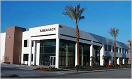 |
Tamarack Scientific Co.,Inc.
220Klug Circle
Corona, CA 92880
USA8
Tel: +1 (951) 17-3700 |
반도체 공정의 꽃이라 불릴 정도로 가장 중요한 핵심 공정인 Lithography 장비 중 Mask Aligner와Spin Coater로 세계적으로 정평이 나 있는 SUSS MicroTec사가 미국 California Corona에 위치한 Tamarack Scientific을 2012년 초에 인수함에 따라 국내에서 20년 넘게 SUSS 장비를 취급해 온 신코가 그간 축적된 우수한 기술력을 바탕으로 Tamarack장비에 대해서도 영업 및 서비스를 담당하게 되었습니다.
1966년에 설립된 Tamarack은 Laser Processing과 Photolithography System의 선도적인 기술 개발로 미국, 유럽은 물론 아시아에많은 장비를 공급하여 왔습니다. 신뢰할 수 있는 Turnkey Solution을제공하는 Tamarack 장비들은 Advanced Packaging, 3D Integration, MEMS, HB-LED, Organic Electronics and Solar등의 반도체 분야에 사용됩니다.
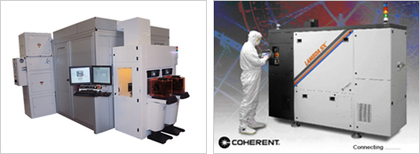
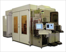
Tamarack사의 Representative Products는Excimer Laser Source를사용한 ELP300과 UV Lamp를 사용하는 Projection Scanner DSC300이 있습니다. ELP300 Series는Excimer Laser Source를 이용하여 Wafer Ablation을진행함으로써 Coating/Develop 및 Etching등의 공정을 생략할 수 있어서 획기적인 공정 시간 단축 및 비용 절감을 달성할 수 있게 합니다. 그리고 DSC300 Series는 Coated Wafer와 Mask 간의 Contact 없이 Expose를 하기 때문에 Mask Contamination이 없으며, Catadioptric Projection Lens를 사용하여Fine Resolution 구현이 가능합니다. 또한, Large DOF로Thin PR 뿐만 아니라 Thick PR에서도 정확한 Image구현이 가능하며, 다양한 NA(Numerical Aperture, 0.07-0.14)값을 이용하여 Resist의 Sidewall Angle의control이가능한 장점을 가지고 있고, Exposure 시 Scanning 방식 채용 및 High Intensity(4000mW/cm2) 적용으로 High Throughput을 얻을 수 있습니다.

I. ExcimerLaser Processing System
Excimer laser system can be used to ablate, anneal, de-bond and expose. Excimer ablation is best described as photo-chemically initiated electron excitation leading to a sudden increase in pressure which results in an explosive removal of material into monomers and gases known as ablation.
ELP300 (ELP Series)
| • |
Resolution to 2um |
| • |
Sub-micron alignment accuracy and high-throughput processing
|
| • |
Large FOV in the industry(Ø100mm)improves throughput by reducing overheads and enabling the creation of large non-repeated patterns
|
| • |
Robotic wafer/substrate loading from FOUP, cassette or conveyor
|
| • |
Dynamic beam measurement and control to ensure accurate execution of
stringent process parameters.
|
| • |
Available wavelengths of 248nm or 308nm utilizing the broadest range of
Excimer lasers in the market
|
| • |
Configurable processing methods which allow for step&repeat, step&scan and continuous scanning to match process requirements
|
| • |
Available manual load option for small batch runs or research applications
|
| • |
SECS/GEMM
|
II. Projection Lithography
Tamarack’s UV projection scanners are engineered for high throughput,maximum yield and low cost of ownership. Image resolution to sub-3microns,and outstanding depth of focus ensures superior imaging in ultra-thick resists.
These advantages when coupled with sub-micron alignment accuracy, makes
these scanners unique in their ability to accurately expose large substrates.
DSC300 (Dyson Scanner)
| • |
Broadband 1:1 catadioptric projection lens provides resolution<3um and a large depth of focus for accurate imaging of both thin and ultra-thick resists
|
| • |
Ability to process wafers/substrates up to 300mmX300mm
|
| • |
High irradiance and excellent beam uniformity from a single UV arc lamp for accurate and economical imaging of a variety of photoresists while maintaining high throughput
|
| • |
Automated alignment to accuracy of less than 1um, utilizing through-the-lens and off-axis vision optics coupled with Cognex’s pattern recognition system |
| • |
Ability to control resist sidewall angles by varying the numerical aperture (0.07-0.14) and focal position at the resist surface |
| • |
Selectable filters for the broadband illumination source and projection lens allow matching of wavelength to the specific resist characteristics |
| • |
Robotic wafer handling from dual FOUP load ports (quad optional)
|
| • |
Automatic 14”/9” mask handling from mask library with capacity for 15 masks
|
| • |
Large projection lens working distance prevents any contact with the wafer |
| • |
Intuitive and flexible control system enables highly customized process automation & SEC/GEMM |

| Tamarack Scientific’s proven systems can help you engineer an application-specific solution. |
|
| • |
Advanced Packaging and 3D integration |
| • |
Organic Electronics |
| • |
Photovoltaics |
| • |
HB-LED |
| • |
MEMS, etc. |
Excimer Laser
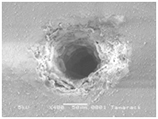
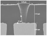
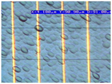
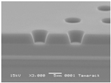
| TMV Drilling |
TSV Blind ViaSiNx Ablation |
|
 |
 |
 |
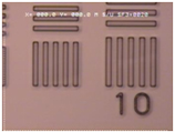
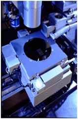
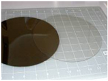
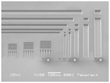
| SU-8 ImagingLaser Debonding |
 |
 |
 |
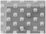
| Vias/InkJet Heads |
Resist Ablation |
 |
 |
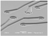
| RDL Trench and Via |
SLR(Seed Layer Removal) |
|
 |
 |
|
|